│靜電消散鍍膜-功能與應用
| 服務項目 | 功能 | 特性說明 | 主要規模 | 應用 | 備註 |
| 靜電消散薄膜 | 靜電防護,減少ESD敏感源漸受到破壞。 | 穩定的表面抗組、高耐磨 | 表面阻抗:106~107 Ω/sq | 1. IC測試用change kid 2.與ESD敏感元件接觸之設備(如:arm , robot ,chuck等) | 預計2016年年底量產 |
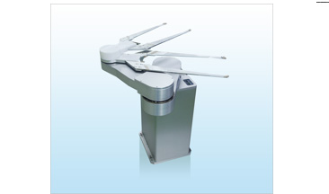
實際產品應用:鍍著於靜電敏感元件之接觸之設備(如:arm, robot, chuck 等) ,避免電荷釋放造成 wafer/ IC 損壞。
靜電消散鍍規格:
| Feature | Thickness | Sheet Resistance | Opertation Temp. | Hardness |
| SPEC | 1-2um | 106~107 Ω/sq | -45~250°C (>250°C under verfication | >8H |
JEDEC 靜電防護規格:
| JESD625B Frequency | JESD625 ITEMS | JESD625-B (2012) Accerptance Limits | ESD S20.20 Accerptance Limits | |
| 4.Recommented Quarterly | a) | ESD protective static dissipative worksurface to ESD ground resistance. (see Note 5) | ≥ 105 to <109 Ω | <1X10⁹ Ω |
| b) | ESD conductive worksurface to ESD ground resistance.(see Note 5) | <105 Ω( with no series resitor) | <1 Ω | |
| c) | ESD protective floor/mat to ESD ground resistance using ANSI/ESD S7.1. | ≥ 105 to <109 Ω | <1X10⁹ Ω | |
| d) | Wrist strap monitior check | ≥ 500kΩ to≤10MΩ <2.0Ω | ||
| e) | ESD ground continuity form the groundable point(e.g mobile equipment grounp wires) using EOS/ESD-S6.1. | <2.0Ω | <1.0 Ω | |
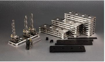
IC傳送冶具
Wafer 傳送手臂